|
Process 2018 |
|
|
Process 2018 |
The entire process of creating a printed circuit board with isolation milling is described.
The operating system is Ubuntu 18.04
Steps:
Design a circuit with KiCAD 5
freerouting
pcb2gcode
Autoleveller AE
cnc.js
KiCAD 5:
http://kicad-pcb.org/download/ubuntu/
freeRouting.jar
source: https://github.com/nikropht/FreeRouting/tree/master/gui
using your previously created user libraries for symbols:
open symbol library editor
Preferences -> manage symbol libraries
click on browse libraries and find your Library
your previously created user libraries for footprints:
open footprint library editor
Preferences -> manage symbol libraries
click on browse libraries and find your Library
Zooming in with the title section enabled makes it difficult to see the diagram when zooming to fit page.
File-> Page Settings
Page layout description file:
empty.kicad_wks
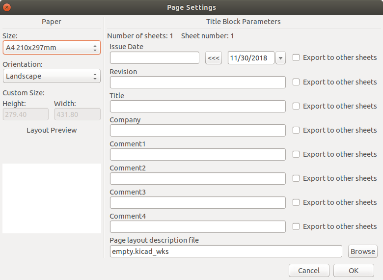
then change page size to smaller
to pan: press and hold F4
move the mouse
Disable red frame with title:
https://forum.kicad.info/t/how-to-disable-red-frame-with-title-etc/11511/2
deselecting the ‘worksheet' box in the render panel.
In layout manager, select edge.cuts
(blue triangle)
![]()
Use Add graphic lines to draw board edge
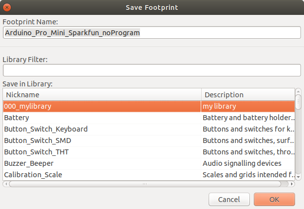
Open footprint editor
File -> Open Footprint
modify footprint as needed
File -> Save
Save in Library allows to choose new library to save in
-Right click on the modified pad -> Pads->Copy pad settings
-Right click on a NON-modified pad you want to modify ->Pads -> Apply (or Push for several) pad settings
https://forum.kicad.info/t/how-do-you-edit-several-pads-at-once-in-footprint-editor/9209
Open KiCAD EESchema (Schematics Editor)
Import Parts
snapEDA
click on generate net list
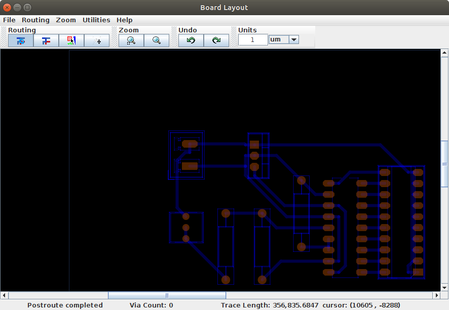
Open KiCAD Pcbnew
load net list
Trace width and spacing
In the process of routing the traces, you may need to delete the existing traces.
wider traces: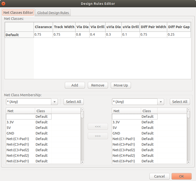
To delete all traces:
Edit -> Global Deletions
KiCAD Pcbnew export DSN Specctra
freerouting import
autoroute
export Specctra session file
KiCAD Pcbnew import session file
Note: When you change rules in KiCAD, those are not considered unless you first delete the rules file in freerouting.
batterymonitor.rules
FreeRouting opens a file chooser in the user's home directory. This adds extra steps every time a design is changed. Improvement?
cp batterymonitor.dsn ~
java -jar ../../../../../../applications/freeRouting/freeRouting.jar batterymonitor.dsn
cp ~/batterymonitor.ses .
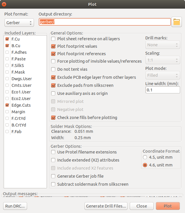
Open KiCAD pcbnew.
File -> Plot
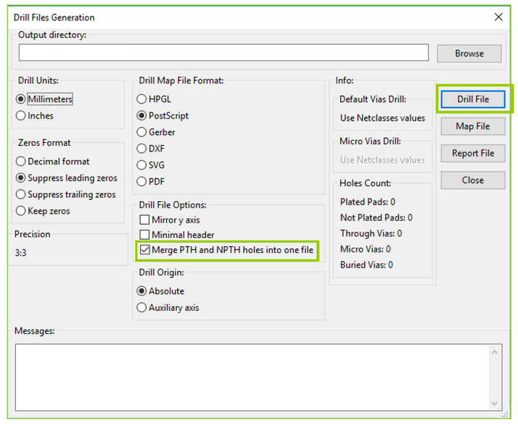
generate a single drill hole file:
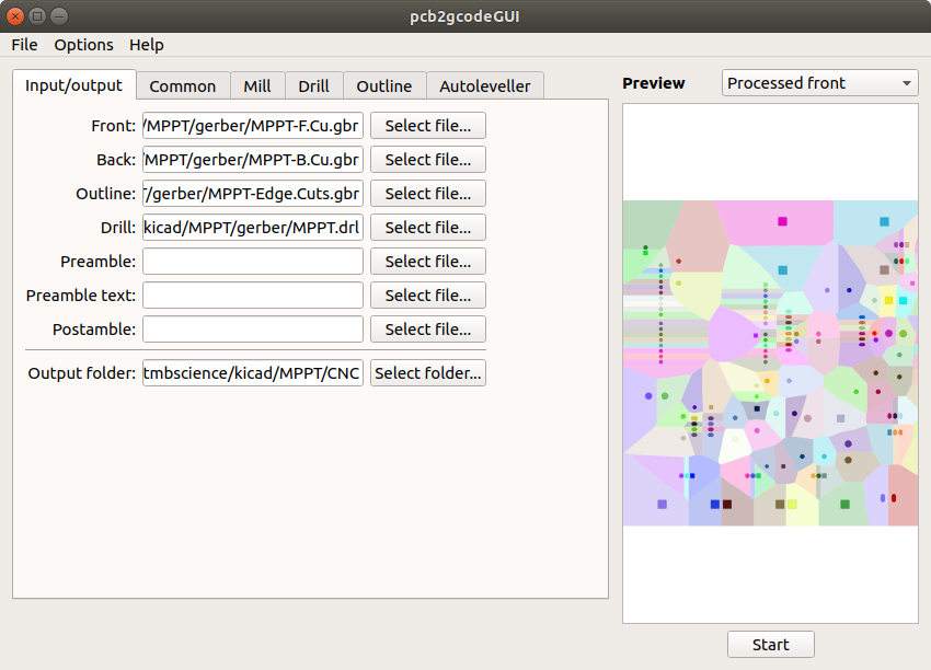
Open pcb2gcodeGUI
Input/output tab:
add front gcode so that mounting holes are drilled
add back gcode with actual traces
add outline so that autoleveller knows offset from board edge for probing grid
add drill file
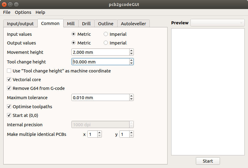
Common tab:
Change Movement height to 2 mmm
Remove G64 (to prevent error in GRBL)
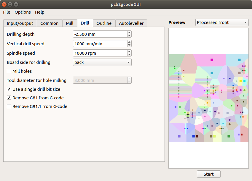
Drill tab:
set "board side for drilling" to back (same as traces)
check single drill bit size to reduce tool change
check "Remove G81" because GRBL and TinyG do not support canned cycles
import your PCB gcode into Autoleveller AE
generate probing gcode with Probe File Generator
run probe file in cnc.js
save probing results as Raw Probe File
load Raw Probe File in Autoleveller AE
generate autolevelled PCB gcode
run autolevelled PCB gcode on your PCB in cnc.js.
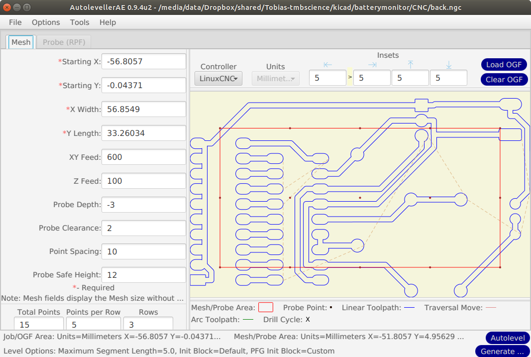
If the physical PCB is exactly the size of the designed board, enter insets so that the probing does not start at the edge of the board.
The probing grid file that is generated by Autoleveller does not work unedited with cnc.js.
Simply remove the initial comment section.
open cnc.js
load gcode
> G64 P0.01000 ( set maximum deviation from commanded toolpath ) (line=26)
error:20 (Unsupported command)
ALARM:1 (Hard limit)
[MSG:Reset to continue]
perhaps electrical issue?
just disable hard limits
$21=0
Sometimes program gets stuck at the end and can only be unlocked by resetting Arduino which is a problem because zero position gets lost.
Solution: Add M0 at the end of the program. When it is reached, don't continue but
Instead, move spindle to zero x and y.
Then stop program.
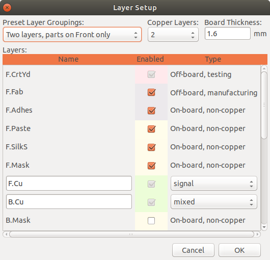
In Pcbnew: Setup -> Layers Setup
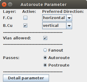
In freeRouting:
Utilities -> Parameter -> Autoroute